


2Research Scholar, Department of ECE, K L University, & Assistant professor, Department of ECE, ALIET, Andhra Pradesh, India
Keywords: Mems; Radio frequency; Switching; Cantilever; Beam; Electrostatic force; Material science
GaAs FET switches do not have sufficient isolations to minimize cross interference and signal jamming from channels is close proximity. Pin diode require considerable power for operate. MEMS switches provide high isolation when isolation loss when open, low insertion loss when closed, and can be operated at low power consumption [3]. The performance of MEMS is good in Radio Frequency [3]. RF MEMS and waveguide technology constitute a very promising solution, since they allow for very high Q and good tunability. They employ tunable components (e.g. varactor diodes) and have the advantage to be very compact, but exhibit unloaded Qs below 100 [4]. MEMS switches provide high isolation, which is required in Base stations and satellite systems [5].
RF MEMS Switches classification depends on type of actuation, deflection axis, contact type, circuit configuration, and Structure configuration (Figure 1).
This paper discusses about electrostatically actuated fixedto- fixed bridge base capacitive and resistive type switches, cantilever based capacitive and resistive switches Shown in the figure. In electrostatically actuated switches the type of forces effects the deformation of the beam are classified as static forces (spring, Electrostatic, Contact force) and dynamic forces (Damping, Inertial force). Electrostatically actuated switches

Fixed-Fixed Beam switch is generally known as shunt switch, and cantilever beam based switches are generally known as series switches. The shunt capacitive switches will provide more than -20dB isolation at 10-50GHz in down state, and -0.04 to -0.1 dB insertion loss at 5-50 GHz in upstate
Where: l- Length; w- Width; t- Thickness; td- Dielectric thickness; g0- Gap between electrodes; W- Width of electrode


Beam Mass (m) = l*w*t*ρ (1)
2. Stress (𝞂): It is defined as the ratio of applied force(F) to area (A) units are in N/m2 i.e.,
Stress (σ) = F / A (2)
3. Strain(ε): After applying some load the beam will deform,stain is used to measure the deformation factor. It is the ratio of deformed length (Δ) to original length of beam (l) and it is constant.
Strain (ε) =Δl / l (3)
4. Elastic Modulus (E): It is derived from Stress(σ) and strain(ε) values, expessed as
Elastic Modulus (E) = σ/ε (4)
5. Area Moment of Inertia(I): In this paper all the theoritical equations are derived by considering the the beam structure is rectangular in shape. And the moment of inertia for rectangular beam is given as
Area Moment of Inertia (I) = (t3w) / 12 (5)
6. Deflection (𝜹): When a significant force is applied on the structur there is defenetly a noticeble deformation will occure in the structure, to measure the deformation deflection is helpful and for rectangular cantilever it is given as
Deflection (δ) = (ql4) / (8EI) (6.1)
7. For a rectangular fixed-fixed beam the deflection is formulated as.
Deflection (δ) = (5ql4) / (384EI) (6.2)
In both the cases, the uniformly distributed load (q) is applied on the structures.
Stiffness (K) = (2EWt3) / (3l3) (7)
\[\sqrt {\frac{K}{m}} \]
3.67 (Vp / Vsω0)
\[\frac{b}{{2\sqrt {Km} }}\] Where: b-Damping Coefficient
Quality Factor (Q) = K/bω0
1. Electrostatic force: when a significant voltage is applied in between electrodes some electrostatic force will create and it can be expressed as
\[\frac{1}{2}\frac{{{\varepsilon _0}A{V^2}}}{{{{\left( {{g_0} + \frac{{{t_d}}}{{\varepsilon r}} - \delta } \right)}^2}}}\] 2. Pull-in Voltage: The basic principle of electrostatic RF MEMS Switch is, some amount of voltage need to apply to get the deformation in the beam for switching. And for the recangular bassed beams the expected pull-in voltage is
\[\sqrt {\frac{{8K}}{{27A{\varepsilon _0}}}{g_0}{{\left( {\frac{{{t_d}}}{{{\varepsilon _r}}}} \right)}^3}} \] 3.Pull-up Voltage: After applying the pull in voltage the beam will deforms and because of elastic property of the beam it will try to get the stability. At waht voltage level the bram try to get the initial position is said to be pull up voltage.and the pull up voltage is formulated as
\[\sqrt {\frac{{2K}}{{A{\varepsilon _0}}}{g_0}{{\left( {\frac{{{t_d}}}{{{\varepsilon _r}}}} \right)}^2}} \] 4. Capacitance: The capaciatnce in RF MEMS Switches is divided as Upstate capacitance and downstate capacitance.
The bridge based capacitive type switch has the Upstate Capacitance (Cu) = Cp + Cpp+Cf, and Down State Capacitance (Cd) = Cp+1.5Cpp+Cf, where Cp-Parasitic capacitance, Cpp-Parallel plate Capacitance (𝞮0Ww / g0), and Cf- Fringing Field Capacitance. Fringing field capacitance which is around 10%-20% of Cpp where: ε0-Free space permittivity = 8.854 x 10⁻¹² F/m [2].
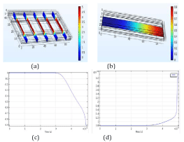
As shown in the (figure 4), a cantilever based switch with geometrical dimensions length l = 90 μm, width w = 20 μm, thickness t = 1 μm, gap between the electrodes go=0.1μm. and the dielectric thickness td =0.9 μm and the width of the bottom electrode W = 20 μm. Gold (Au) is used as a cantilever material, and Silicon Nitride (Si3N4) with dielectric constant 7.5 is used as dielectric material. And the working principle of the switch is, initially the input applied voltage is 1mv there is no deformation in the switch under this condition input is equal to output, but the second case in addition a 5v is added to 1mv then there is some electrostatic force is created between the electrodes then the cantilever will deform and touches to ground under this condition the output is zero.
With the above mentioned dimensions and working principle an electrostatically actuated capacitive switch is designed and simulated using Comsol Multiphysics FEM tool, the results are shown in (Figure 5).
A. Material Selection:
1) Wafer: Most of the MEMS devices fabrication takes the substrate as silicon, GaAs, Quartz, as active substrates and polymers, Plastic, Ceramics, are as passive substrates.

3) Dielectric: Silicon Dioxide(Sio2), Silicon Nitride (Si3N4), Polymethyle Methacrylate (PMMA).
4) Sacrificial Layer: the material used as sacrificial layer must and should consist some mechanical properties like adhesion and low residual stress to avoid failures in the switch. So the selection of structural material and the sacrificial layer combination is very important. Few combinations are shown in (Table 1).
a. Cleaning: After completion of each fabrication step, followed by there is cleaning process will present to remove dust particles. Piranha cleaning is famous for wafer cleaning after completion of each step.
b. Piranha Cleaning: The combinaation of sulfuric acid (H2SO4):Hydrogen peraxide (H2O2) is used as cleaning solution for wafer and some tiems used to remove photoresist.
c. Masks preparation:Generally RF MEMS Switch fabrication require transmission layer mask, dielectric mask, sacrificial layer mask, beam or membrane mask, overall minimum four masks require for lithography [8].
d. Photo Lithography: This process is used to remove the unwanted portion from the deposited film. In this process fist a photoresist layer is uniformly formed on the surface of the film with the help of spin coater. Generally PMMA, PMGI are used as photoresist material. Next UV light is projected on the photoresist through a mask, and after by using developers the exposed (Positive) or unexposed (negative) photoresist is removed by using different developers as shown in (Figure 6).
e. E. UV Light: Generally PMMA, PMGI, DQN are used as positive photoresist and Bis (aryl)azide rubber, KTRF are used as negative resist materials. Positive resist materials are more sensitive to UV light, and negative resist materials are more sensitive to electron beam.
f. Deposition Techniques:In micro fabrication, different type of materials like semicondutors, metals, poly silicon, dielectrics need to diposit on the wafers for that there different dipocition techniques are available. The diposition techniques are classification is shown in the (Table 2).
g. Etching: Removal of specified portion with the help of chemicals or gases is known as etching in micro fabrication process. Etching processes classification is shown in the (Table 3).
Structural Material |
Sacrificial Material |
Poly Silicon, Gold, Aluminum, etc. |
SiO2, Phosphosilicate Glass (PSG) |

Deposition Techniques |
|||
Thermal Oxidation |
Physical Vapor Deposition |
Chemical Vapor Deposition |
Others |
Wet Oxidation |
- Evaporation (Thermal / E-Beam) |
-PECVD |
-Electroplating |
Cantilev: In this section the fabrication of a SiO2 cantilever on silicon wafer using bulk micromachining is explained.
(a) As the basic step, the wafer is cleaned using piranhasolution (H2SO4:H2O2 in 9:1 ratio) to remove the organic and chemical contaminations on the wafer surface, rinse with DI water and blower with nitrogen. After cleaning the wafer samples are forwarded to thermal oxidation to form the SiO2 on the Silicon wafer surface. As the next step in photolithography, first the samples are dehydrated at 250°C for 10 minutes. Next a photoresist (PMMA) is formed on the surface of the samples by using a spin coater with 4000 rpm for 10 sec. Soft baking is the intermediate process of keeping the samples at 95°C for 2 minutes to evaporate the solvents in the photoresist. (b) And next UV light is exposure through a cantilever mask for 2 sec. (c) After UV exposure the samples are placed in a special developing solution (NAOH) which will dissolve the exposed photoresist, rinse with DI water and blower with nitrogen processes will follow. (d) Now the exposed SiO2 is removed using BHF based wet etching. (e) Acetone Solution is used to remove the leftover photoresist and again the piranha cleaning using H2SO4:H2O2 in 3:1 ratio, DI water clean nitrogen blow is done to remove the dust particles. (f) Next the exposed silicon is etched isotropic ally using KOH.
J. Surface Micromachining: In surface micromachining the entire structure of the element is created on the top of the substrate as shown in the (Figure 9).
h. Cantilev: In this section the patterning of a simple Silicon cantilever beam using Silicon on Insulator (SOI) wafer by following surface micromachining process is explained.
(a) As the basic step, the SOI is cleaned using piranha solution (H2SO4:H2O2 in 9:1 ratio) to remove the organic and chemical contaminations on the wafer surface, rinse with DI water and blower with nitrogen. A Positive Photoresist Material (PMMA) is formed on the surface of the SOI by using a spin coater with 4000rpm for 10 sec. Soft baking is the intermediate process of keeping the samples at 95°C for 2 minutes to evaporate the solvents in the photoresist. (b) Next the coated SOI is forwarded to photolithography; here first the samples are dehydrated at 250°C for 10 minutes and UV light is exposure through a cantilever mask for 2 sec. (c) After UV exposure the samples are placed in a special developing solution (NAOH) which will dissolve the exposed photoresist, rinse with DI water and blower with nitrogen processes will follow. (d) Now the exposed Si is removed using dry etching like anisotropic plasma etching. (e) Piranha cleaning to remove the leftover photoresist using H2SO4:H2O2 in 3:1 ratio, DI water clean nitrogen blow is done to remove the dust particles. In the cleaning process petri dishes are used to carry the solutions. (f) Next the samples are place in wet etch BHF solution to remove the exposed SiO2 and to release the cantilever. Finally the samples are dried up to critical point to avoid the stiction and to prevent the structural collapse.
i. UV Light: Alternatively there exist one more fabrication method i.e. LIGA Process, but it is costly and complex compared to Surface and bulk micromachining processes.
Etching Processes |
|
Wet Etching |
Dry Etching |
Immersion Etching |
Plasma Etching |


Switch Type |
Problems |
Metal Contact Switch |
- Increasing Contact Resistance |
Capacitive Coupling Switch |
- Stiction between the dielectric layer and the metal |
Other than the packaging the major challenges are reduction of pull-in voltage, humidity and temperature tolerance, stiction, lifetime, Structure Viscoelastic Problems.
- Gabriel M R, Jeremy B. M, RF MEMS Switches and Switch circuits. ISSN 1527-3342/01/$10.00Ó; 2001. IEEE microwave magazine.
- Laurent D, Member, Rebeiz G M. Intermodulation Distortion and Power Handling in RF MEMS Switches, Varactors, and Tunable Filters. ieee transactions on microwave theory and techniques. 2003; 51(4).
- Mercado L L, Kuo S M, Lee T Y, Russell Lee. Analysis of RF MEMS Switch Packaging Process for Yield Improvement. IEEE transactions on advanced packaging. 2005;28(1).
- Luca P, Fabrizio C, Paola F, Roberto S. High- Tunable Waveguide Filters Using Ohmic RF MEMS Switches. ieee transactions on microwave theory and techniques. 2015;63(10).
- Muldavin J B, Rebeiz G M. All-Metal High-Isolation Series and Series/Shunt MEMS Switches. IEEE Microwave and Wireless Components Letters. 2001;11(9).
- Bakri-Kassem M, Mansour R R. High Power Latching RF MEMS Switches. ieee transactions on microwave theory and techniques. 2015;63(1).
- Barbato M, Gaudenzio M. A Novel Technique to Alleviate the Stiction Phenomenon in Radio Frequency Microelectromechanical Switches. IEEE electron device letters. 2015;36(2).
- Hijazi Y S, Hanna D, Fairweather D, Vlasov Y A, Grover L L. Fabrication of a Superconducting MEM Shunt Switch for RF Applications. IEEE transactions on applied superconductivity. 2003;13(2).
- Zhen P, Cristiano P, James C M H, David I F, Charles L G, Cody M, et al. Impact of Humidity on Dielectric Charging in RF MEMS Capacitive Switches. IEEE microwave and wireless components letters. 2009;19(5).
- Kaan D, Erdem Y, Simsek D, Tayfun A. A New Temperature-Tolerant RF MEMS Switch Structure Design and Fabrication for Ka-Band Applications. journal of microelectromechanical systems. 2016;25(1).
- Jaehong P, Eun S S, Wooyeol C, Youngmin K, Youngwoo K, Dong-il C, A Non-Contact-Type RF MEMS Switch for 24-GHz Radar Applications. journal of microelectromechanical systems. 2009;18(1).

